en:pfw:spi_gd32vf_noforth
Table of Contents
SPI protocol for the GD32VF103
- Bitbang on port-A
Note that the highlevel generates a 300 kHz clock, the low level variant a 1 MHz clock. The bitbang SPI setup has no restrictions at all. More on I/O-ports from page 101ff of the user manual mentioned below. - Hardware SPI on port-A The upper limit of the SPI clock of the GD32 is 27 MHz, so always check your settings. With noForth you may add the SPI setup routine to the APP vector. The first version of SPI-setup did not initialise the NSS pin, thanks to Martin Bitter & Wolfgang Strauss this is corrected. More on SPI from page 377ff of the user manual.
 Read a character using SPI from a W25Q64 external Flash memory
Two examples
| File name | Commands | Purpose |
|---|---|---|
| SPI-loopback.f | COUNTER | A counter as simplest loopback test |
| Flash driver GD32.f | SPI-ON | Activate SPI-interface to W25Q64 Flash memory chip |
FILL1 0 write-sector | Fill buffer with pattern en write to Flash sector 0 | |
0 100 FDUMP | Dump sector 0 showing the written contents, etc. | |
| SPI OLED display GD32.f | DEMO | Initialise OLED & display P-F-W until a key is hit |
&PAGE | Erases the OLED and sets the cursor in upper left corner |

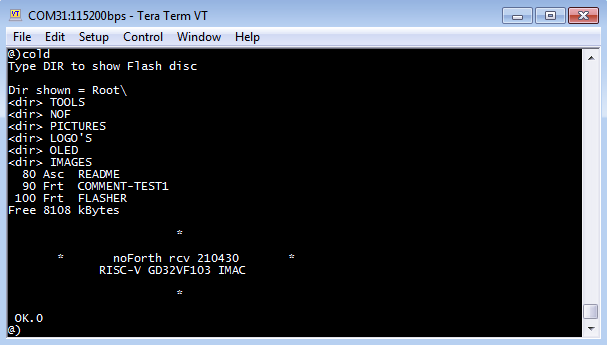
NOF filesystem on SPI Flash initialised while booting the GD32VF103
More information on the GD32VF103
- Datasheet, GD32VF103 Datasheet Rev 1.3.pdf
- User manual, GD32VF103 User Manual EN V1.2.pdf
en/pfw/spi_gd32vf_noforth.txt · Last modified: by 54.36.148.211
